

Reliable PCB Assembly: Key Factors for Flawless Electronics Production
2026-10-06
Every flawless device starts long before the first solder melts. It starts with a PCB assembly process that treats reliability not as a checkbox, but as the default setting. At TPS, we’ve watched small oversights in pad design, component placement, or thermal profiling quietly sabotage production runs. This post unpacks the factors that separate boards that last from boards that fail—without the fluff.
Soldering Flaws That Quietly Kill PCB Reliability
A board that passes final test can still fail weeks later because a cold solder joint finally gives way under repeated thermal cycling. The joint looks fine from the outside—shiny, full fillet—but inside the intermetallic layer never formed properly. That hairline fracture grows every time the board heats up and cools down, eventually turning an intermittent reset into a dead product. No amount of rework fixes a joint that was starved of heat or flux from the start.
Head-in-pillow defects on BGA packages are another stealth killer. The ball and paste both melt, but they don't actually merge; they just touch, leaving a weak connection that passes electrical test at room temperature. Similarly, voiding under QFN thermal pads traps gas that expands during operation, slowly lifting the component away from the board. You won't see these with a magnifying glass, and they rarely show up until the product has been in the field for months.
Fine-pitch bridging and tombstoning of small passives are more visible but still overlooked during fast inspection. A solder bridge between two adjacent pins might be hidden under a component body, and a tombstoned resistor can sit there with one end soldered and the other lifted just enough to break contact under vibration. These flaws share a common thread: they degrade slowly, mask themselves as software glitches, and quietly erode the reliability you thought you built in.
How Component Sourcing Decisions Shape Flawless Boards
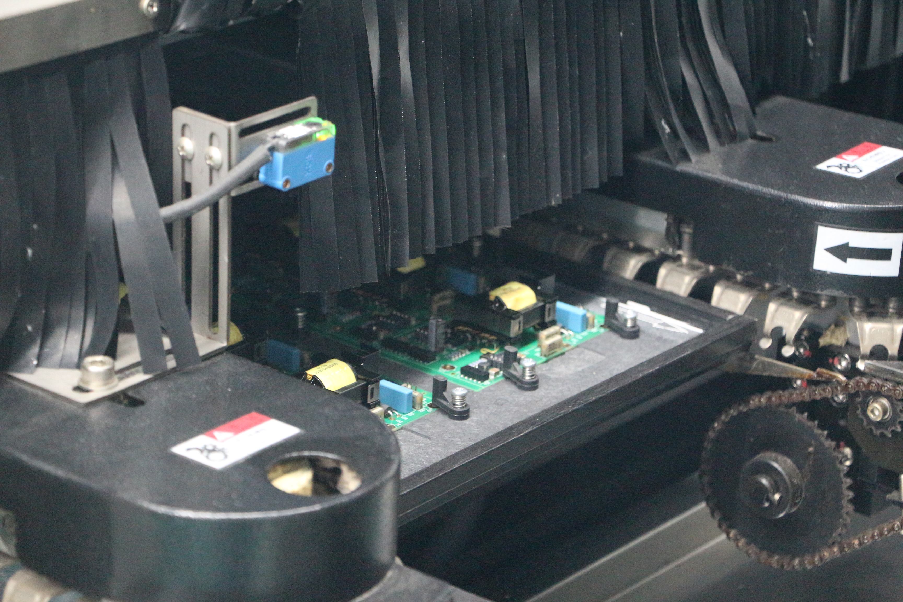
Every flawless board starts long before solder touches copper. It begins with a quiet vetting of distributors, lot codes, and moisture-sensitive packaging. A single counterfeit regulator or a batch of capacitors that barely meets tolerance can turn a promising design into a field failure report. Engineers who ignore sourcing variability often spend weeks chasing phantom signal integrity issues that actually trace back to inconsistent dielectric materials or off-spec solder masks.
The real leverage comes from treating sourcing as a design constraint rather than a procurement afterthought. When you lock in a limited set of approved passives and connectors early, you eliminate most of the impedance mismatches and thermal surprises that show up during bring-up. But flawless boards also demand a second look at lifecycle data: a component that works beautifully on a bench today can disappear from the market in eight months, forcing a rushed substitution that compromises pad geometry or reflow profiles.
In the end, sourcing decisions shape not just the bill of materials, but the margin for error in every solder joint and signal path. Boards built from tightly controlled lots with traceable origins tend to survive temperature cycling and mechanical stress without the subtle fractures that plague cheaper, mixed-batch assemblies. That difference rarely appears on a datasheet—it shows up in the absence of late-night debugging and the confidence to ship without caveats.
Thermal Cycles and the Stress Points You Overlook
Most discussions around thermal cycling focus on the obvious culprits—solder joints, connectors, or large ceramic capacitors. But the real failures often start in places that never show up on a thermal camera. Thin traces near mounting holes, for example, act as fuses for mechanical stress. Each heating and cooling cycle pulls them microscopically, until a hairline crack interrupts a signal you assumed was rock solid.
via stitching is another silent victim. Designers treat vias as purely electrical shortcuts, forgetting that copper expands nearly twice as much as the surrounding laminate. Over hundreds of cycles, that mismatch turns every barrel into a tiny piston. The plating thins from the inside out, and intermittent opens appear only after the board reaches a specific temperature.
Edge connectors and press-fit pins hide the same problem in plain sight. The gold plating masks the underlying stress until a cold morning brings a field return. Instead of adding more thermal relief, look at the board as a set of competing expansion rates. Move a few critical traces away from high-strain regions, increase annular ring size on vias near heat sources, and double-check that your mechanical standoffs aren't fighting the PCB's natural breathing.
Inspection Points Most Assembly Lines Skip Too Early
Most lines still run a full end-of-line check, but by then a loose connector or an untorqued bracket is buried under three other modules. The real trouble starts at stations one through five: fixturing pins that aren’t checked for wear, first-off torque values that get recorded only if someone remembers, and harness clips that feel seated but aren’t locked. These early points don’t get a dedicated inspector because the line is still “warming up,” yet that’s exactly when drift sneaks in.
Skipping them doesn’t save time—it moves the cost downstream. A misaligned bracket caught at station six means popping off side covers and rerouting a harness. A connector half-seated before the console goes in can pass every later voltage test and still fail in the field. The cheap fix is a ten-second check at each of the first three stations: mark torque witness lines, use a simple go/no-go block for pin height, and add a click test for connectors before the next part covers them.
These are not extra inspections; they’re precorrections. Once you start logging the first-hour rejects by station, the pattern becomes obvious—most of them trace back to the same two or three fasteners and one alignment boss. Fix those and the end-of-line failure rate drops without adding labor.
DFM Adjustments That Prevent Costly Rework Later
Too many design teams treat manufacturability as a checklist item at the end of the cycle, only to watch tooling costs balloon when a simple fillet or draft angle was never applied. Early DFM adjustments—like setting minimum wall thickness around bosses, avoiding deep pockets that demand long-reach cutters, or standardizing hole sizes to reduce tool changes—don't just make the part cheaper to produce. They keep the design stable enough that you aren't forced into a redesign after the first article inspection reveals warpage, sink marks, or fit issues that could have been flagged in CAD.
The expensive rework usually starts small: a tolerance stack that looked fine on the drawing but causes interference in assembly, a surface finish specified as SPI A-1 that requires five extra hours of hand polishing per cavity, or a snap-fit feature that cracks because the gate location wasn't moved away from the high-stress area. Addressing these in the design phase costs almost nothing—a quick conversation with the mold maker, a thirty-minute simulation, or swapping a material to one with a documented shrink rate. Waiting until the steel is cut means paying for EDM adjustments, re-polishing, or even recutting entire inserts, all while your production schedule slips.
Practical DFM adjustments that pay off later include adding simple draft to all vertical walls, not just cosmetic surfaces; keeping ribs under 60% of the nominal wall thickness to avoid sink; and locating parting lines away from sealing surfaces or visible areas. Also worth checking: whether your design actually needs that threaded insert, or if a molded-in boss with a self-tapping screw would do. Each change is small, but together they prevent the kind of late-stage feature creep that turns a two-week tooling lead time into a two-month rescue effort.
Material Mismatches That Undermine Electronics Longevity
Designers often treat each material in isolation, signing off on a substrate’s dielectric constant or a solder’s melting point without checking how the pair behaves over thousands of thermal cycles. A ceramic board paired with a thick copper pour may look fine on the bench, but once the assembly sees real temperature swings, the difference in expansion rates turns every interface into a micro-shear test. The result isn’t always a dramatic crack; more often it’s a slow delamination that quietly raises resistance until a trace opens under load.
Electrochemical potential differences can be just as damaging. When tin-based solder meets a gold flash over nickel, humidity provides the electrolyte for a tiny corrosion cell. The gold itself stays intact, but the underlying nickel dissolves over time, leaving a brittle, high-resistance layer that field technicians call black pad. Repairs won’t stick, and intermittent faults become the norm rather than the exception.
Even supposed matches, like crimped copper terminals on aluminum wire, degrade without the right interlayer. Aluminum’s higher creep rate and rapid oxidation reduce contact force, which raises joint temperature and accelerates further oxidation. The fix is rarely a stronger connector; it’s recognizing that material interfaces, not just material strengths, determine how long a product survives outside the lab.
FAQ
A dependable process hinges on tight control of solder paste quality, component placement accuracy, and thermal profiling. If any of these drift, you end up with intermittent connections or boards that fail early.
Because improper heat can crack solder joints or delaminate components without showing immediate defects. A carefully tuned reflow profile is what keeps every joint solid even when the board later faces vibration or temperature shifts.
Substrates with higher glass transition temperatures and finishes like ENIG resist oxidation and mechanical stress far better than cheap laminates. Thin copper or low-grade laminates often lead to pad lifting and broken traces after a few thermal cycles.
AOI systems compare each board to a golden reference and flag misaligned parts, insufficient solder, or tombstoning in real time. This catches process drift early enough to fix the line before entire batches are compromised.
Flux residues and microscopic contaminants can create leakage currents or corrosion over time, especially in humid environments. Proper cleaning and handling remove these slow-acting reliability killers that don't show up in initial tests.
Cold solder joints from uneven heating, wrong component orientation due to poor programming, and using expired solder paste are frequent culprits. Each can pass basic testing but degrade under real-world vibration or temperature swings.
They run first-article inspections, cross-section samples to check solder joint integrity, and subject boards to thermal cycling or burn-in tests. Only after these pass do they lock the process parameters.
Look for documented process controls, traceability of every batch, and the willingness to share yield data. A partner who treats assembly as an engineering discipline rather than a commodity service will catch issues before they reach your production line.
Conclusion
Even small soldering defects, like a slightly cold joint or a micro-void under a BGA, can lie dormant until thermal cycling turns them into open circuits. Pair that with component sourcing that chases the cheapest parts without locking down traceability, and you've already set the stage for field failures. The boards that survive years of use are the ones where engineers treat every pad and every reel as a potential weak link. They know that mismatched solder paste chemistries or a laminate with the wrong glass transition temperature will flex and crack under normal operating heat. Thermal cycles are relentless; they don't care if the stress concentrates at a via barrel or a connector pin. The difference between a flawless run and a quiet reliability nightmare often comes down to whether you designed those stress points out before the first board hit the line.
Most assembly lines wait until after reflow to catch problems, but by then a tombstoned 0201 or a shifted QFN has already committed the board to rework or scrap. The lines that consistently ship reliable product push inspection earlier, checking stencil prints and placement data before the oven gets a chance to bake in the mistakes. That same mindset applies to design for manufacturability: a footprint that looks fine on a CAD screen can cause solder bridging or insufficient fillet when the stencil and pick-and-place tolerances stack up. And it's not just about geometry. Material mismatches, like a component finish that fights the flux system or a conformal coating that traps moisture against a sensitive IC, will slowly undermine longevity even if every solder joint looks perfect under AOI. Flawless electronics production isn't a single checkpoint; it's a chain of decisions where each weak link shows up later as a customer return.
Contact Us
Contact Person: Lily
Email: [email protected]
Tel/WhatsApp: +49 (0) 2161 49526-0
Website: https://tps-elektronik.com/en/